Microstructural analysis is essential in semiconductor manufacturing for evaluating thin films, wafer cross-sections, and complex multilayer structures. Challenges include sectioning ultra-thin substrates, preserving delicate interfaces, and achieving mirror-flat surfaces for defect analysis and failure of investigation. Allied High Tech Products meets these demands with advanced solutions like the X-Prep® Precision Polishing System, designed for controlled material removal and high-accuracy planarization. Combined with our grinding and polishing workflows, X-Prep ensures repeatable, artifact-free surfaces — delivering the precision required for today’s semiconductor research and production.
Do you need an industry-specific technical application report?
Ceramic Resistors
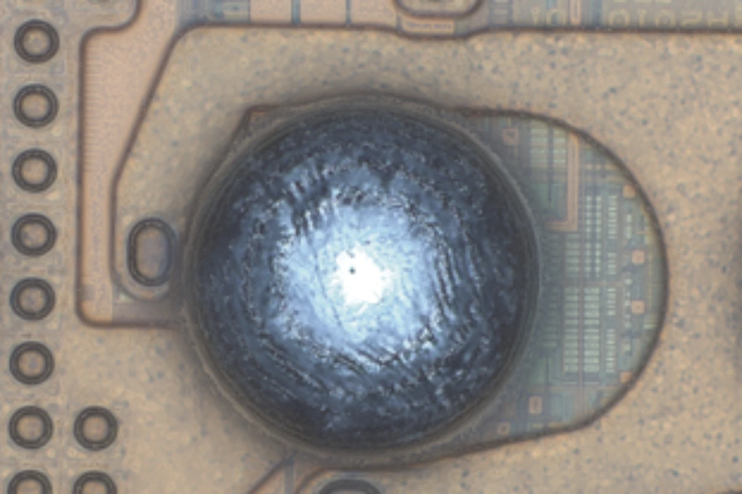
Coated Gold Bond Wire Cross-Sections
Electronic Device
Electronic Devices with Silicone
LED Cross-Sections
Packages on a Circuit Board
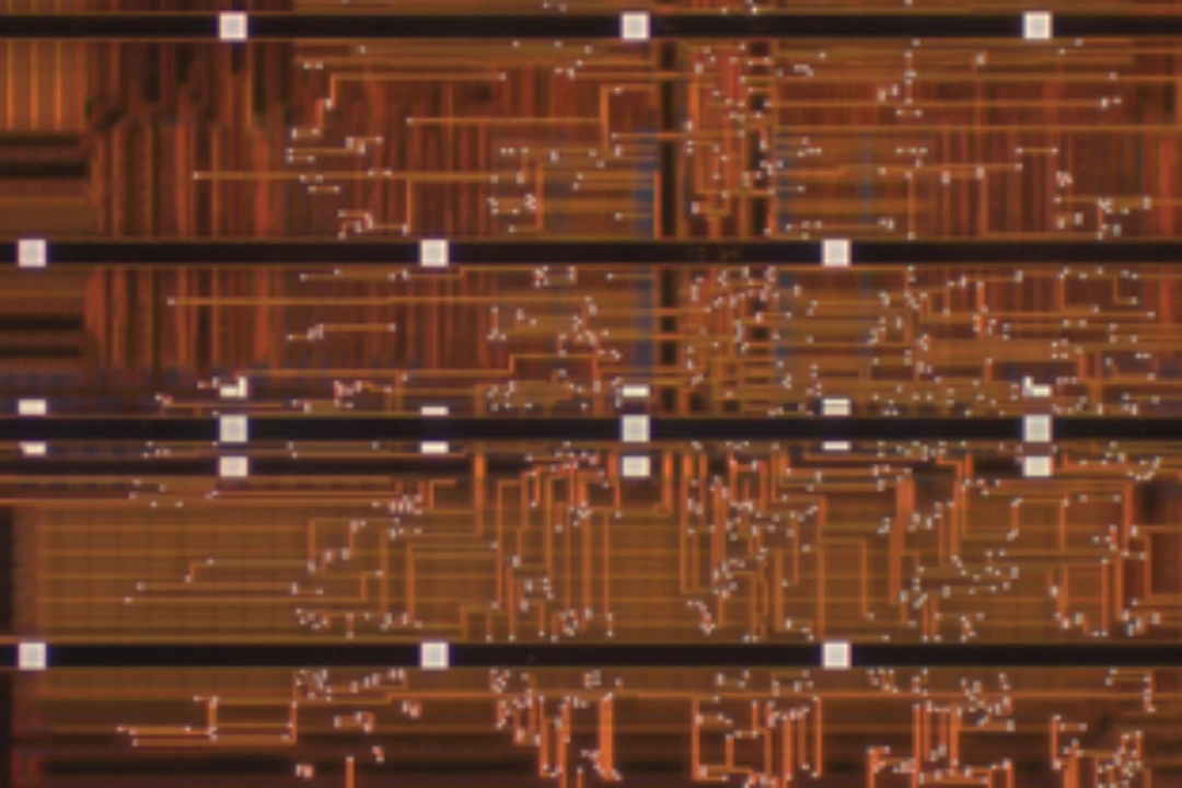
Parallel Lapping Integrated Circuits
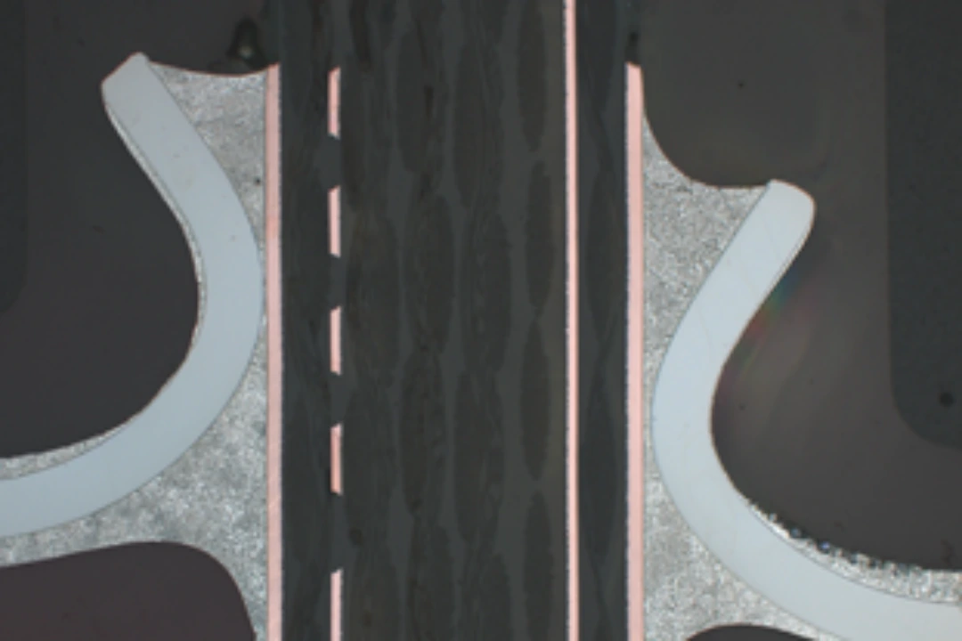
Silicon Angle Cross-Section Small Package Cross-Section